
Projects
Ongoing Projects
SPRINTER: Low-coSt and energy-efficient hybrid Photonic integrated circuits for
fibeR-optic, free-space optIcal and mmWave commuNication systems supporting Time
critical networking in industrial EnviRonments
[September 2022 – February 2026]
PCRL coordinates the SPRINTER Project. SPRINTER will provide a set of low-cost, energy-efficient, and ultra-dynamic optical transceivers and an optical switching solution to cope with the diverse needs of the industrial networks and expedite their truly digital transformation. SPRINTER will combine the best-of-breed optical components and methods from various powerful but complementary photonic integration platforms to develop low-cost and energy-efficient 200 Gb/s optical transceivers, and ultra-fast wavelength-tunable 10 Gb/s optical transceivers. Leveraging well-proven integration techniques that allow for the fabrication of complex 3D photonic integrated circuits, the project will provide a disruptive low-loss and polarization-insensitive reconfigurable optical add-drop multiplexer, optimized for operation within space-division multiplexing networks. Considering the ultra-dynamic nature of the industrial networks due to the deployment of either temporarily fixed or moving remote nodes, SPRINTER will provide a set of groundbreaking photonics-enabled transceivers supporting wireless connectivity by means of a free-space optical or a mmWave channel. The transceivers will be able to operate reliably in indoor environments, as well as, outdoor environments thanks to the complementary characteristics of the two channels. The project will also develop a unified network platform, providing the required methods and tools to support time-deterministic operation, and enable real-time communication with guaranteed service quality. In order to showcase SPRINTER’s full potential, the developed technology will be evaluated within application scenarios that will be deployed in a relevant industrial environment incorporating a fully operational closed-loop control system.

LOLIPOP: Lithium NiObate empowered siLIcon nitride Platform
for fragmentation free OPeration in the visible and the NIR
[September 2022 – February 2026]
PCRL coordinates the LOLIPOP Project. Despite the huge progress by photonics, extended spectral bands at wavelengths below 1100 nm remain heavily underserved in terms of integration solutions. At the same time, the silicon nitride is booming and the lithium niobate is making an impressive comeback in the form of lithium niobate on insulator (LNOI), with both materials being transparent both in the visible and the NIR. With all these viewed as a unique opportunity, LOLIPOP steps in to develop a disruptive platform that will offer the highest integration, modulation and second order nonlinear performance in the entire spectrum from 400 up to 1600 nm, based on the combination of the LNOI and the silicon-nitride (TriPleX) technology. To this end, LOLIPOP will develop die-bonding and microtransfer-printing methods for low-loss (<0.5 dB) integration of LNOI films on TriPleX without compromise in the functionality of the two platforms. It will also develop a process for growth of Ge photodiodes (PDs) inside pockets and a process for flip-chip bonding of active elements inside recesses on TriPleX. Given the possibility of the Ge-PDs to operate in the entire 400-1600 nm spectrum, and the flexibility of the bonding process to adapt to different actives and wavelengths, the picture of this ultra-wideband technology is complete. LOLIPOP will demonstrate its potential via the development of: 1) The first ever integrated laser Doppler vibrometer at 532 nm with ultra-narrow linewidth (<5 kHz) and ultra-high modulation (6 GHz), 2) The first ever integrated FMCW-LIDAR at 905 nm with ultra-high linear chirp (10 GHz) and optical phased array-based 2D beam scanning, 3) Photonic convolutional neural networks with record scale, computation speed (24 TOPS) and power consumption reduction compared to electronic solutions, and 4) The first ever integrated squeezed-state source with 6 dB squeezing level for quantum applications at 1550 nm. A roadmap for the offering of LOLIPOP technology as commercial service will be prepared.
AEOLUS: an Affordable, miniaturisEd, clOud-connected system powered by
deep Learning algorithms for comprehensive air qUality measurements based
on highly integrated mid-IR photonic
[January 2021 – December 2023]
PCRL coordinates the AEOLUS Project. AEOLUS, leveraging on the experience of its partners on novel photonic components (e.g. broadband thermal emitter, graphene photodetector), will demonstrate in an operational environment (TRL 7) an affordable, miniaturised, multi-gas (10 – 15 gases) sensor based on highly integrated photonic chips in the mid-IR (3 μm – 10 μm). AEOLUS sensors will be cloud connected, deployed in an existing IoT testbed, while the plethora of data acquired will be used to develop deep learning algorithms for chemometric analysis. AEOLUS sensing system will demonstrate the calculation and accurate prediction of indoor and outdoor air quality, greenhouse gases concentration, and toxic gas leakages detection. The sensing system will provide many functionalities for the end-user such as real-time alerts, notifications, visualized reports and overlays while it will allow taking automatic actions where they are needed. AEOLUS will also demonstrate how user engagement can be promoted through its system, employing gamification concepts and incentivise the end users. AEOLUS targets for a cheap portable sensor, tested for its interoperability, with many functionalities and quality of life services, targeting a very wide range of applications to ensure its widespread deployment. The proliferation of the AEOLUS sensor in the community acts in an exponential manner (leveraging Big Data techniques and Deep Learning algorithms), further enhancing the system’s accuracy and speed. AEOLUS sensing system is completely in line with its industrial partners’ roadmaps and exploitation plans and it is foreseen to have a product in the market 0-2 years from the end of the project. Ultimately, the acquired data and analysis will be made available to policy-makers and stakeholders, so that AEOLUS has a far-reaching impact in EU’s citizens life.
PICaboo: Photonic Integrated Circuits on InP technology plAtform enaBling
low cost metro netwOrks and next generation PONs
[January 2021 – December 2023]
PCRL coordinates the PICaboo Project. Cloud applications, 5G and IoT are pushing modern networks over the edge to satisfy the stringent high capacity and low latency demands. Photonic integration is a key enabling technology to tackle the new challenges and to bring new products and services to the market. PICaboo will develop novel building blocks on the InP PIC platform of TUe and III-V Lab based on the generic foundry model aiming to enhance PIC performances and reduce development costs. It will develop compact models of the building blocks and will compile them in PDK-compatible libraries allowing designers to explore their use in a wide range of applications hence maximizing their exploitation potential. PICaboo PIC demonstrators will transform the optical metro and access networks in terms of speed, footprint, power consumption and cost. The high speed EAM-based transmitters will employ all-optical equalization functionality on-chip which will scale PON line rate to 50/100Gb/s reducing the electronic signal pre-processing required for meeting the 29dB power budget of the optical distribution network within the expected dispersion limit. Both single EAM-MZM and coherent EAM-IQM transmitter PICs will leverage power consumption benefits of 50 and 65% respectively compared to 50G EML solutions and overall cost reduction by almost 20%. The dual polarization coherent receiver PIC employs integrated reset-free phase and polarization control allowing for complex DSP functions to be performed directly at the optical domain. In this case, power consumption reduction of more than 30% with concurrent cost benefits 3.6x will be achieved compared to standard coherent transceivers stemming from the use of simplified direct detection DSPs and low-cost tunable lasers, making PICaboo an attractive technology within the 20-80km DCI range. Exploitation of the PIC demonstrators will be pursued by NOKIA and ADVA. VLC will exploit the developed PDK libraries for a fast uptake of PICaboo building blocks by end-users.
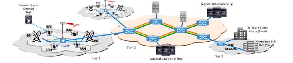
Int5Gent: Integrating 5G enabling technologies in a holistic service
to physical layer 5G system platform
[November 2020 – October 2023]
PCRL coordinates the Int5Gent Project. Int5Gent targets the integration of innovative data plane technology building blocks under a flexible 5G network resource, slice and application orchestration framework, providing a complete 5G system platform for the validation of advance 5G services and IoT solutions. The project builds upon a suite of innovative 5G technological solutions spanning hardware, software, and networking systems that have been conceptualized and developed under the latest 5GPPP initiative projects and are now taken to TRL-7 and above. It also combines novel and state-of-the-art solutions able to further upgrade the capabilities and maturity level of cutting-edge 5G core technologies enabling the creation of an innovative 5G ecosystem. A sample of the developed and offered technologies include flexible multi-RAT baseband signal processing, beam steering, mmWave technology solutions at 60GHz and 150GHz bands, hardware-based edge processor with TSN, GPU processing capabilities, innovative 5G terminals and elastic SDN-based photonic data transport. The integration of the technology blocks is performed as part of an overall 5G architecture that promotes edge processing and is orchestrated by an NFVO compatible framework with edge node extensions at the network layer and an overlay vertical services application orchestrator at the user plane layer. The overall platform is implemented in two extended testbeds which include actual field deployed segments and managed by the network operators of the consortium. The validation and showcasing testbeds host 3 use case scenarios covering the deployment of services related to multiple vertical sectors as well as innovative applications for smart IoT networked devices. The use cases are designed in order to highlight the benefits of the adopted technologies in terms of increased bandwidth, low latency and high reliability and create new markets opportunities especially for the participating SMEs through pilot validation of their offered solutions.

PhotonHub Europe: One-Stop-Shop Open Access to Photonics
Innovation Support for a Digital Europe
[January 2021 – April 2025]
PCRL participates in PhotonHub Europe Project. PhotonHub Europe will establish a single pan-EU Photonics Innovation Hub which integrates the best-in-class photonics technologies, facilities, expertise and experience of 53 partners from all over Europe, including the coordinators of EU pilot lines and local photonics hubs representing 18 regions, as a one-stop-shop solution offering a comprehensive range of supports to industry for the accelerated uptake and deployment of photonics. PhotonHub will provide European companies, in particular “non-photonics” SMEs and mid-caps that are first users and early adopters of photonics, with open access and guided orienteering to the following key support services: training and upskilling opportunities within PhotonHub’s Demo and Experience Centres throughout Europe and enhanced by digital tools for online learning; “test before invest” innovation support capabilities to engage with companies on highly collaborative Innovation Projects aimed at TRL acceleration from prototyping (TRL3-4) to upscaling (TRL5-6) to manufacturing (TRL7-8), and complemented by targeted business and IP advisory supports; and support to find investment through investment-readiness coaching and investor match-making organised in collaboration with major regional and European venture fora and deep tech Investor Days. PhotonHub will uniquely support cross-border innovation activities of European companies, while simultaneously working closely with the local photonics hubs to develop and roll out best practices of the “lighthouse” regions for ongoing regional financial support of SME innovation activities and to support the creation of new innovation hubs covering most regions of Europe. Finally, PhotonHub will fine-tune and implement its business plan for long-term sustainability in the form of the PhotonHub Europe Association as a durable entity which is deeply rooted within the wider ecosystem of local, regional and EU-DIHs for maximum leverage and impact on European competitiveness and sovereignty.

Int5Gent: Integrating 5G enabling technologies in a holistic service
to physical layer 5G system platform
[November 2020 – October 2023]
PCRL coordinates the Int5Gent Project. Int5Gent targets the integration of innovative data plane technology building blocks under a flexible 5G network resource, slice and application orchestration framework, providing a complete 5G system platform for the validation of advance 5G services and IoT solutions. The project builds upon a suite of innovative 5G technological solutions spanning hardware, software, and networking systems that have been conceptualized and developed under the latest 5GPPP initiative projects and are now taken to TRL-7 and above. It also combines novel and state-of-the-art solutions able to further upgrade the capabilities and maturity level of cutting-edge 5G core technologies enabling the creation of an innovative 5G ecosystem. A sample of the developed and offered technologies include flexible multi-RAT baseband signal processing, beam steering, mmWave technology solutions at 60GHz and 150GHz bands, hardware-based edge processor with TSN, GPU processing capabilities, innovative 5G terminals and elastic SDN-based photonic data transport. The integration of the technology blocks is performed as part of an overall 5G architecture that promotes edge processing and is orchestrated by an NFVO compatible framework with edge node extensions at the network layer and an overlay vertical services application orchestrator at the user plane layer. The overall platform is implemented in two extended testbeds which include actual field deployed segments and managed by the network operators of the consortium. The validation and showcasing testbeds host 3 use case scenarios covering the deployment of services related to multiple vertical sectors as well as innovative applications for smart IoT networked devices. The use cases are designed in order to highlight the benefits of the adopted technologies in terms of increased bandwidth, low latency and high reliability and create new markets opportunities especially for the participating SMEs through pilot validation of their offered solutions.

SEER: A “Smart” Self-monitoring composite tool for aerospace composite manufacturing using Silicon photonic multi-sEnsors Embedded using through-thickness
Reinforcement techniques
[January 2020 – December 2022]
PCRL coordinates the SEER Project. SEER is an Innovation Action that aims to develop smart self-monitoring composite tools, able to measure process and material parameters and, thus, to provide real-time process control with unprecedented reliability. SEER consortium will achieve this by:
1) developing miniature photonic sensors,
2) embedding those sensors in the tool with through-the-thickness techniques which minimise
alteration of the structural integrity of the tool itself and
3) optimising the manufacturing control system through the implementation of a prototype process monitoring, optimisation, and process control unit.
SEER will adopt a multi-sensor approach that will comprise a temperature, a refractive index, and a pressure sensor, operating in the near infrared and all integrated on a miniature photonic integrated circuit (PIC). The SEER solution will be compatible with and optimise existing composite manufacturing methods and its reuse for several resin curing cycles will increase efficiency and save resources. The embedded PIC sensors in a reusable tool will cater perfectly to address preprocessing and will use acquired raw data for process optimisation, using theoretical models and machine learning algorithms, establishing for each tool a link between the sensor data, material state models, process parameters, as well as degradation of the tool. This will allow efficient preventive maintenance of the tool with less effort and provide insight on better tool design. Finally, the acquired data from quality testing of cured parts will be used to optimise the process control ensuring further enhance in the quality yield and will provide with a part quality fingerprint.

NEBULA: Neuro-augmented 112Gbaud CMOS plasmonic transceiver
platform for Intra- and Inter-DCI applications
[January 2020 – December 2022]
PCRL participates in NEBULA Project. NEBULA aims to provide the foundations for a common future-proof transceiver technology platform with ultra-high bandwidth capabilities offered by a CMOS compatible toolkit and tailored towards meeting performance, cost and energy metrics in both inter-DCI coherent and intra-DCI ASIC co-packaged optics. NEBULA will be investing in the established bandwidth- and energy saving credentials of plasmonic modulator solutions together with the functional digital processing portfolio of neuromorphic optical reservoir computing engines towards painting the landscape of the next-coming disruption in transceiver evolution, tailoring them in System-in-Package prototype assemblies that can intersect with the challenging framework of both inter- and intra-DCI segments. NEBULA target to demonstrate i) a fully-functional 8-channel 112Gbaud 16QAM C-band transceiver prototype, offering an aggregate capacity of 3.2Tbps and requiring just 2.65W per single 400Gbps wavelength, providing in this way an energy efficiency of only 6.625pJ/bit with energy savings of 93% compared to current 200Gbps and 19W-consuming pluggable optics and ii) a fully-functional sub-Volt 8-channel 112Gbaud PAM4 O-band transmitter co-packaged with a data generating ASIC from Mellanox, offering a 1.6Tbps aggregate capacity with up to 37% energy savings compared to the estimated power requirements of respective Si-photonic-based co-packaged solutions.

POETICS: CoPackaging of Terabit direct-detection and coherent Optical Engines
and switching circuits in mulTIChip moduleS for Datacenter networks and the
5G optical fronthaul
[January 2020 – December 2022]
PCRL coordinates the POETICS Project. POETICS is a H2020 Research and Innovation project funded by the European Union aiming to bring the optical interconnect technology with all performance, functionality and cost credentials and allow the Datacenter (DC) networks to scale and the 5G wired infrastructures to grow. Enabling terabit-capacity optical interconnects requires a paradigm shift in the packaging approach. The electrical interconnect distance between the optical engine (OE) and the digital switching chip must be minimized, signal conditioning chips and unwanted components, like sockets that would otherwise be required and would inevitably lead to increased power consumption and reduced signal integrity, should be removed. It also requires the right combination of photonic and electronic technology to be integrated in order to deliver high performance, low-cost and energy efficient optical engines. POETICS will develop novel Terabit optical engines and optical switching circuits and co-package them with digital switching chips to realize Multi-Chip Modules (MCM) for next generation switching equipment with >12.8 Tb/s capacities and very high energy efficiency that fit into the roadmap of vendors. In order to achieve these goals POETICS will utilize SiGe BiCMOS, InP, PolyBoard and TriPleX technologies and rely on hybrid integration, which allows the selection and combination of the best performing components. The specific targets in POETICS are to develop: • MCM with 1.6 Tb/s OEs based on 8-fold InP-EML arrays (200 Gb/s per lane) and PolyBoard with parallel SMFs on par with the PSM/DR spec for 500 m – 2 km intra-DC connectivity; • MCM with 1.6 Tb/s OEs based on 8-fold InP-EML arrays (200 Gb/s per lane) and 3D PolyBoard with duplex MCFs for 5G optical fronthaul applications; • low-power-consumption 3D Benes optical switch; • MCM coherent 64 Gbaud OEs with up to 600 Gb/s capacity of DC interconnect applications within 80 – 120 km reach on par with 400G-ZR specification.
TWILIGHT: Towards the neW era of 1.6 Tb/s System-In-Package transceivers for datacenter appLIcations exploiting wafer-scale co-inteGration of InP membranes
and InP-HBT elecTronics [December 2019 – November 2023]
PCRL coordinates the TWILIGHT Project. IoT, 5G and cloud applications have created a huge growth of datacentre traffic fuelling the market of 400GbE and the ratification of 800GbE and 1.6T standards expected within 2013-2015. Datacentre operators must keep pace with the increasing speeds and to cope with the increasing power consumption required for airflow management and cooling. Moreover, they must address the massive interconnectivity between servers and switches dictated by 5G ultra-low latency applications. 100Gb/s per lane is the next step for the realization of 800GbE modules but this will be the end of pluggables and the start of co-packaged optics with ASICs paving the way to 1.6T and beyond. TWILIGHT aims to bring InP membranes and InP-HBT electronics at unprecedently close distances (<20um) to unleash the speed capabilities of its high performance components and to enable 112Gbaud per lane. Wafer-scale bonding together with high-accuracy assembly and co-packaging concepts, TWILIGHT’s optoelectronic engines will be capable of up to 1.6T capacity. Selective area growth will be exploited to develop C-band and O-band EMLs and UTC photodiodes in combination with echelle gratings on the same system-on-chip platform. Adaptation of the SAG layerstack will be used to develop polarization insensitive SOAs enabling complex functionalities on chip. TWILIGHT will leverage analog bandwidth interleaving for interfacing its transceivers with next generation 112G SERDES and will develop analog (de)multiplexers, >110GHz linear drivers and 100GHz TIAs. TWILIGHT will exploit the PI-SOAs to develop 4×4 and16x16 optical space switches exhibiting nanosecond latency and >50% smaller footprint. The O-band and C-band SiP transceiver demonstrators leverage up to 72% and 74% power consumption savings compared to established technologies and target the datacentre market (2-10km) and DCI (<40km), respectively, with estimated cost 0.89€/Gb/s. Exploitation of TWILIGHT’s technologies is aimed via its industrial partner MLNX.
5G-COMPLETE: A unified network, Computational and stOrage resource Management framework targeting end-to-end Performance optimization for secure 5G muLti-tEchnology and multi-Tenancy Environmentsand InP-HBT elecTronics
[December 2019 – November 2023]
PCRL coordinates the 5G-COMPLETE Project. 5G-COMPLETE aims to revolutionize the 5G architecture, by efficiently combining compute and storage resource functionality over a unified ultra-high capacity converged digital/analog Fiber-Wireless (FiWi) Radio Access Network (RAN). By employing the recent advances in Ethernet fronthauling introduced by the eCPRI standard as a launching point, 5G-COMPLETE introduces and combines a series of key technologies under a unique architectural proposition that brings together i) the high capacity of fiber and high-frequency radio, ii) the audacity of converged FiWi fronthauling, iii) the spectral efficiency of analog modulation and coding schemes, iv) the flexibility of mesh self-organized networks, v) the efficiency of high-speed and time-sensitive packet-switched transport, vi) the rapid and cost-efficient service deployment through unikernel technology and finally vii) an enhanced security framework based on post-Quantum cryptosystems. 5GCOMPLETE’s proposed converged Computing/Storage/RAN infrastructure effectively merges the 5G New Radio fronthaul/midhaul/backhaul faculties into one common Ethernet-based platform and transforms the RAN into a low-power distributed computer that shapes new network concepts. 5G-COMPLETE’s results will be validated in a range of scalable lab- and fieldtrial demonstrators in Athens (Greece), Lannion (France) and Bristol (UK). Upon completion, 5G-COMPLETE will have introduced new business models and novel research opportunities that will be streamlined into tangible results by its 13 consortium partners that expand along the complete 5G research and market chain.
TERAWAY: Terahertz technology for ultra-broadband and ultra-wideband operation of backhaul and fronthaul links in systems with SDN management of network
and radio resources
[November 2019 – October 2022]
PCRL coordinates the TERAWAY Project. TERAWAY is a H2020 5GPPP Phase III project funded by the European Union coming as a technology intensive project aiming to develop a disruptive generation of THz transceivers for high-capacity BH and FH links in 5G networks.
Leveraging optical concepts and photonic integration techniques, TERAWAY will develop a common technology base for the generation, emission and detection of wireless signals with selectable symbol rate and bandwidth up to 25.92 GHz within an ultra-wide range of carrier frequencies covering the W-band (92-114.5 GHz), D-band (130-174.8 GHz) and THz band (252-322 GHz). In this way, TERAWAY steps into providing for the first time the possibility to organize the spectral resources of a network within these bands into a common pool of radio resources that can be flexibly coordinated and used. The use of photonics will enable the development of multi-channel transceivers with amplification of the wireless signals in the optical domain and with multi-beam optical beamforming in order to have a radical increase in the directivity of each wireless beam. In parallel, aiming to take the most out of the THz technology and enable its commercial uptake, the project will develop a new software defined networking (SDN) controller and an extended control hierarchy that will perform the management of the network and the radio resources in a homogeneous way with obvious benefits for the network performance and energy efficiency and with possibilities for the provision of network slices in order to support heterogeneous services. At the end of this development, TERAWAY will make available a set of ground breaking transceiver modules including 4-channel modules operating from 92 up to 322 GHz, with possibility to offer 241 Gb/s total data rate, to have more than 400 m transmission reach in the THz band (and few Km in the lower bands), and with 4 wireless beams that can be independently steered and establish BH and FH connections between fixed terrestrial and moving network nodes. The TERAWAY transceivers will be evaluated at the 5G demo site of AALTO and NOKIA in Finland, under an application scenario of communication and surveillance coverage of outdoor mega-events using moving nodes in the form of heavy-duty drones.
ACTPHAST 4R: Accelerating Photonics Deployment via one Stop Shop Advanced Technology Access for Researchers
[January 2019 – December 2023]
PCRL participates in ACTPHAST 4R project. ACTPHAST 4R is a unique one-stop-shop photonics technology access and support centre for European researchers which is perfectly aligned with their needs in bridging the gap between fundamental research at TRL1-2 and applied research up to TRL4-5. Driven by the deployment ambitions and capabilities of a critical mass of European top-class researchers -in particular non-photonics researchers for whom advanced photonics is a key enabling technology to the realisation of so many exciting and diverse new applications and products, ACTPHAST 4R will directly support the accelerated deployment of existing cutting-edge photonics technologies by providing them with action-oriented solutions on two complementary levels. In the first instance, ACTPHAST 4R will provide researchers with one-stop-shop access to the photonics expert know-how and mature technologies of 24 of Europe’s leading competence centres. The photonics technology platform capabilities of ACTPHAST 4R cover the entire integrated supply chain from design to packaging. Through intensive technology coaching, leading to focused innovation projects involving transnational internships and hands-on working with the advanced photonics technologies at the host institutes, the goal is to turn the researchers’ scientific conceptual breakthroughs into industrially relevant demonstrators. In parallel, ACTPHAST 4R will provide researchers with expert business coaching to help foster their entrepreneurial mindset and deployment capabilities, with guidance to pathways for further scaling of their demonstrators and financing of innovation in the industrial domain. Ambitious targets are set for commercial valorisation successes by “star performing” researchers in the form of patents, licensing deals and spin-outs. As a result, ACTPHAST 4R will be a game-changer in strengthening the European innovation ecosystem and improving the cross-fertilisation of photonics with other technology areas.
TERIPHIC: Fabrication and assembly automation of TERabit optical transceivers based on InP EML arrays and a Polymer Host platform for optical InterConnects up to 2 km
and beyond
[January 2019 – March 2023]
PCRL coordinates TERIPHIC project. Efforts to develop optical interfaces with Terabit capacity for datacom applications have kicked off. A practical path to the Terabit regime is to scale the current 400G modules, which are based (in the most forward looking version of the standards) on 4 parallel lanes, each operating with PAM-4 at 53 Gbaud. Scaling these modules by adding lanes looks simple, but entails challenges with respect to the fabrication and assembly complexity that can critically affect their manufacturability and cost. TERIPHIC aims to address these challenges by leveraging photonic integration concepts and developing a seamless chain of component fabrication, assembly automation and module characterization processes as the basis for high-volume production lines of Terabit modules. TERIPHIC will bring together EML arrays in the O-band, PD arrays and a polymer chip that will act as the host platform for the integration of the arrays and the wavelength mux-demux of the lanes. The integration will rely on butt-end-coupling steps, which will be automated via the development of module specific alignment and attachment processes on commercial equipment. The optical subassembly will be mounted on the mainboard of the module together with linear driver and TIA arrays. The assembly process will be based on the standard methodologies of MLNX and the use of polymer FlexLines for the interconnection of the optical subassembly with the drivers and the TIAs. Using these methods, TERIPHIC will develop pluggable modules with 8 lanes (800G capacity) and mid-board modules with 16 lanes (1.6T capacity) having a reach of at least 2 km. Compared to the 400G standards, the modules will reduce by 50% the power consumption per Gb/s, and will have a cost of 0.3 Euro/Gb/s. After assembly, the modules will be mounted on the line cards of MLNX switches, and will be tested in real settings. A study for the consolidation of the methods and the set up of a pilot assembly line in the post-project era will be also made.

UNIQORN: Affordable Quantum Communication for Everyone: Revolutionizing
the Quantum Ecosystem from Fabrication to Application
[October 2018 – September 2021]
PCRL participates in UNIQORN project. Quantum communication is recognised as one of the pillars for the second quantum revolution thanks to its unique potential for information-theoretical data security. Turning this promise into tangible assets depends however, on the availability of high-performance, compact and cost-effective modules for practical implementations. UNIQORN is a well-orchestrated design and manufacturing framework aiming to advance the quantum communication technology for DV and CV systems by carefully laying out each element along the development chain from fabrication to application. Component-wise, UNIQORN will leverage the monolithic integration potential of InP platform, the flexibility of polymer platform and low-cost assembly techniques to develop quantum system-on-chip modules in a cheap, scalable and reproducible way. UNIQORN will deliver bright (10M pairs/s/mW/THz) heralded, entangled and squeezed light sources with 70-fold size reduction and almost 90% cost savings, room-temperature arrayed SPADs and a 10-GHz CV receiver with low-noise TIAs. Fully functional systems based on these assets will include: (i) a network adapter card with integrated real-time QRNG engine, (ii) the first DPS transmitter as pluggable SFP module for low-cost 1-kb/s QKD, and (iii) novel oblivious transfer and quantum FPGA systems. Network-integration and system evaluation in real fibre networks will be enabled by quantum-aware software defined networking and field trials in the live Smart-City demonstrator Bristol-is-Open. The power of the developed ecosystem will be also validated by pushing current QKD-centric work into higher grounds, and demonstrating one-time programs and secure database access through oblivious transfer. The trans-disciplinary approach of UNIQORN brings together leading European players from quantum optics and photonics enabling to move from lab science to field deployment and bridge the quantum divide between large (governmental) and small (residential) end-users.
QAMeleon: Sliceable multi-QAM format SDN-powered transponders
and ROADMs Enabling Elastic Optical Networks
[January 2018 – October 2022]
PCRL coordinates QAMeleon project. Sustained 2-digit growth in internet traffic is raising the need for new photonic technologies enabling Petabit/s network capacities, whereas suppressed operator margins call for new concepts to make these networks more efficient. QAMeleon aims at a holistic solution towards scaling metro/core networks to the next decade. A new generation of SDN-programmable photonic components, modules and subsystems will be delivered, employing sliceability as a means of optimizing resource utilization and cutting operator costs by >30%.
At the transponder side, QAMeleon will develop components for 2 generations ahead: Operating at 128 Gbaud, they will bring significant savings in footprint (>13×), energy/bit (10.4×) and cost/bit (>4.3×). At the ROADM side, QAMeleon will develop large-scale flex-grid wavelength-selective switches (1×24 WSS) and transponder aggregators (8×24 TPA), reducing footprint and cost/port by more than 40% and 28% respectively, with energy savings per ROADM node reaching 4×. Addressing the emerging needs of 5G network backhaul and datacenter interconnect (DCI) metro-access networks where dynamicity is pivotal, QAMeleon will develop an integrated flex-grid 1×4 WSS with nanosecond-scale switching time. The fast 1×4 WSS will be scalable to large channel counts (i.e. full C-band) and will enable savings in footprint, energy consumption and cost by 20×, 11.5× and 36% respectively.
QAMeleon will integrate its innovative photonic components into functional subsystems: A 3 Tb/s sliceable bandwidth-variable transponder (S-BVT), a flexible ROADM with large-scale WSSs and TPAs, and a fast ROADM for metro-access. All necessary SDN software extensions, plugins and application interfaces will be developed, providing a complete functional SDN framework for the sliceable “white box” subsystems. QAMeleon’s devices will be integrated with the SDN software and validated in scalable demonstrators at Nokia’s lab infrastructure and on TIM’s deployed regional network fiber plant.
3PEAT: A3D Photonic integration platform based on multilayer PolyBoard and TriPleX technology for optical switching and remote sensing and ranging applications
[January 2018 – June 2021]
PCRL coordinates 3PEAT project. 3PEAT will develop a powerful photonic integration technology with all size, functionality and quality credentials in order to help a broad range of optical applications like optical switching and remote sensing, to achieve a strong commercial impact. In order to do so, the project will introduce a fully functional 3D photonic integration platform based on the use of multiple waveguiding layers and vertical couplers in a polymer technology (PolyBoard), as a means to disrupt the integration scale and functionality. Moreover, 3PEAT will combine this powerful 3D photonic technology with a silicon-nitride platform (TriPleX), via the development of a methodology for the deposition and processing of multilayer polymers inside etched windows on TriPleX chips. In parallel with the development of this hybrid 3D technology, 3PeaT will bring a number of key innovations at the integration and component level relating to: a) the heterogeneous integration of PZT films on TriPleX platform for development of phase shifters and switches for operation up to 50 MHz, b) the development of a disruptive external cavity laser on the same platform with linewidth less than 1 kHz, c) the development for the first time of an integrated circulator on PolyBoard with isolation more than 25 dB, and d) the development of flexible types of PolyBoards for the purpose of physical interconnection of other PICs. This enormous breadth of innovations can remove the current limitations and unleash the full potential of optical switching and remote sensing and ranging applications. The main switching module that will be fabricated will be a 36×36 optical switch with 20 ns switching time and possibility for power and cost savings of almost 95% compared to standard electronic solutions. The main sensing module on the other hand will be a disruptive Laser Doppler Vibrometer (LDV) with all of its optical units, including its optical beam scanning unit, integrated on a very large, hybrid 3D PIC.

ACTPHAST 4.0: ACceleraTing PHotonics innovAtion for SME’s: a one STop-shop-incubator
[November 2017 – October 2021]
PCRL participates in ACTPHAST 4.0 project. ACTPHAST 4.0 is a unique “one-stop-shop rapid prototyping incubator” for supporting photonics innovation by European companies, which is financially supported by the European Commission under Horizon2020. ACTPHAST will support and accelerate the innovation capacity of European companies by providing them with direct access to the expertise and state-of-the-art facilities of Europe’s leading photonics research centres (24 ACTPHAST 4.0 partners), enabling companies to exploit the tremendous commercial potential of applied photonics. ACTPHAST 4.0 provides the full spectrum of technology platforms ranging from fibre optics and micro optics, to highly integrated photonic platforms (7 technology platforms), with capabilities extending from design through to full system prototyping. ACTPHAST 4.0 has taken care to ensure that all European companies (big and small but particularly targeted at SMEs) can avail of timely, cost-effective, and low risk photonics innovation support. The aim is to capitalise on the extensive range of capabilities of ACTPHAST 4.0 partners to impact across a wide range of industrial sectors, from communications to consumer-related products, and life sciences to industrial manufacturing. The access of European companies to ACTPHAST 4.0 capabilities will be realised through focused innovation projects executed in relatively short timeframes with a critical mass of suitably qualified companies with high potential product concepts. Furthermore, through its extensive outreach activities, the programme will ensure there is an increased level of awareness and understanding across European industries of the technological and commercial potential of photonics, especially amongst the first users and “non-photonics” end users industries. PCRL participates in ACTPHAST 4.0 in a three-fold manner: (i) as technology provider in photonics telecom, datacom and free space domains; (ii) one appointed member (Prof. Avramopoulos) in the Technical Coordination Team (TCT) of ACTPHAST and (iii) formal representative of ACTPHAST’s outreach activities in the area of Greece, Cyprus, Israel and Turkey.
5G-PHOS: 5G integrated Fiber-Wireless networks exploiting existing photonic technologies for high-density SDN-programmable network architectures
[September 2017-August 2021]
PCRL participates in 5G-PHOS project. 5G-PHOS aims to architect and evaluate 5G broadband wireless networks for dense, ultra-dense and Hot-Spot area use cases drawing from recent results in the area of optical technologies towards producing and exploiting a powerful photonic integrated circuit technology toolkit. It aims to streamline advances in multi-format and multi-bitrate optical communications, in InP transceiver, in Triplex optical beamformers and in integrated optical add/drop multiplexers in order to migrate from CPRI-based towards integrated Fiber-Wireless (FiWi) packetized C-RAN fronthaul supporting massive mmWave MIMO communications.It will deliver: a) a set of SDN-programmable units, called FlexBox and FlexBox-Pro, that will be compatible with the emerging 25Gb/s PON access networks and can deliver FiWi traffic ranging between 25-400Gb/s, b) a set of three different 64×64 MIMO Remote Radio Head configurations exploiting analog optical beamforming and producing 25Gb/s,100Gb/s and 400Gb/s wireless data-rates, c) an integrated FiWi packetized fronthaul for supporting Medium-Transparent Dynamic Bandwidth Allocation mechanisms and cooperative radio-optical beamforming, d) a converged FiWi SDN control plane for optimally orchestrating both the optical and the wireless resources. These blocks will be integrated towards architecting 5G networks for 3 use cases, evaluating their performance in lab-scale and field-trial experiments: a. 25Gb/s peak data rate PON-overlaid 5G FiWi network for dense areas, capable to offer densities up to 1.7 Tb/s/km2 , to be demonstrated also in field-trial experiments at the deployed network of Greek operator COSMOTE. b. 400Gb/s peak data-rate SDM-enabled 5G FiWi network targeted for ultra-dense environments and being capable of offering densities up to 28 Tb/s/km2 with <1msec latency. c.100Gb/s peak data-rate WDM-enabled 5G FiWi network targeted for Hot-Spot areas and being evaluated in field-trial experiments at the stadium of P.A.O.K. F.C. in Thessaloniki, Greece.

Completed Projects
BIOCDx: A miniature Bio-photonics Companion Diagnostics platform
for reliable cancer diagnosis and treatment monitoring.
[January 2017-September 2020]
PCRL coordinates BIOCDx project. Current diagnostic options for cancer treatment monitoring rely on imaging techniques and cannot guarantee proper assessment of therapeutic response. This project aims to develop a disruptive Point of Care (PoC) device for cancer early diagnosis and treatment monitoring as a companion diagnostics tool. One of the scientific breakthroughs of this project is the development of a “cancer stem cells” detection platform by virtue of expression of the cancer stem cell-specific transcription factor TWIST1, which controls the expression of the bloodstream circulating biomarkers like POSTN. Cancer stem cells represent the most aggressive/tumorigenic cell compartment within tumors. BIOCDx will combine advanced concepts from the photonic, nano-biochemical, micro-fluidic and reader/packaging platforms aiming to overcome limitations related to detection reliability, sensitivity, specificity, compactness and cost issues. BIOCDx will rely on ultrasensitive, photonic elements based on an array of 8 asymmetric MZI waveguides fabricated by TriPlex technology on silicon nitride substrates and will achieve a 100 fold improvement –with respect to current technologies- of sensitivity (<10-8 RIU). BIOCDx will employ a smart concept of signal multiplexing for lowering the number of photodetectors required in multi-analyte detection and allowing for a substantial reduction of chip size. A sandwich assay, enhanced with nanoparticles, will be developed, based on the use of two antibodies per protein, to detect all three circulating proteins. This will enhance the limit of detection (LOD) close to femtomolar and the reliability. BIOCDx photonic, nano-biochemical, fluidics and packaging platforms will be integrated into a portable, desktop PoC device. Its validation in preclinical and clinical setting will be performed in three cancer types: breast cancer, hormone-independent prostate cancer and melanoma.


Website
www.biocdx.eu

Watch Video

Dr. Christos Kouloumentas
PICs4ALL: Photonic Integrated Circuits Accessible to Everyone
[January 2016 – June 2019]
PCRL participates in the PICs4ALL CSA project, which aims to increase the impact of photonics and enable access to advanced photonic integrated circuit (PIC) technologies for academia, research institutes, SMEs and larger companies. PICs4ALL will establish a European network of Application Support Centres (ASCs) in the field of PIC technology to connect PIC-development infrastructure throughout Europe. The main task of the ASCs is to lower the barrier to Researchers and SMEs for applying advanced PICs, and thus to increase the awareness of the existence of the worldwide unique facility provided by JePPIX (InP and TriPleX PIC design, manufacturing, testing and packaging). PICs4All ASCs actively support users in taking full advantage of the PIC-technology and its deployment in existing and new applications. To achieve its vision the project combines the two targets of an EC supported CSA, i.e. enabling the access to advanced design, fabrication and characterisation facilities, and stimulating the innovation potential of users, especially SMEs, by supplying hands-on support in developing their business cases.
PCRL will serve as one of the eight ASCs in PICs4ALL, serving users mainly from the geographical area of south-eastern Europe and Eastern Mediterranean. As such, PCRL will actively scout opportunities for the use of PICs in new and existing applications, will promote the use of photonics technology platforms, increase the load of the foundries and support interested users with feasibility studies, design, testing and interface to the foundries.
HAMLET: Heterogeneous Advancement and hybrid integration of polymer
and tripLEx platform for Integrated Microwave PhoTonics
[December 2015 – May 2019]
PCRL coordinates HAMLET. The new generation of broadband microwave systems in various fields (wireless communications, satellite communications, sensing, medical imaging) and especially the emerging 5G wireless technology, have very high requirements in terms of carrier frequency, bandwidth, dynamic range, size, power consumption, tunability, and immunity to electromagnetic interference. In parallel, when the microwave signals that need to be processed have a very high carrier frequency, the integrated circuits should be able to offer high-bandwidth modulation and detection. The combination of these requirements is very challenging, and the necessary photonic integration technology that could exploit the full potential of MWP technology is still missing. Towards that end, HAMLET aims to develop a powerful photonic integration technology, tailored for the first time to the needs of MWP and that will enable the corresponding discipline to meet the expectations for commercial uptake with the advent of 5G era. HAMLET will rely on the heterogeneous integration of graphene sheets on polymer and PZT layers on low-loss Si3N4/SiO2 platforms, so as to develop very fast graphene based electro-absorption modulators and an extensive optical beam forming network. With this hybrid technology HAMLET will develop transceivers to seamlessly interface the optical fronthaul and radio access at the remote antenna units (RAUs) of 5G base stations.
Website
www.ict-hamlet.eu
Watch Video
Dr. Panagiotis Groumas
NEPHELE: eNd to End scalable and dynamically reconfigurable oPtical arcHitecture
for application-awarE SDN cLoud datacentErs
[February 2015 – January 2018]
PCRL is coordinating NEPHELE project, developing a dynamic optical network infrastructure for future scale-out, disaggregated datacenters. NEPHELE’s end-to-end solution extends from the datacenter architecture and optical subsystem design, to the overlaying control plane and application interfaces. NEPHELE builds on the enormous capacity of optical links and leverages hybrid optical switching to attain the ideal combination of high bandwidth at reduced cost and power compared to current datacenter networks.
A fully functional control plane overlay is being developed, comprising a Software-Defined Networking (SDN) controller along with its interfaces. The southbound interface abstracts physical layer infrastructure and allows dynamic hardware-level network reconfigurability. The northbound interface links the SDN controller with the application requirements through an Application Programming Interface. NEPHELE’s innovative control plane merges hardware and software virtualization over the hybrid optical infrastructure and integrates SDN modules and functions for inter-datacenter connectivity, enabling dynamic bandwidth allocation based on the needs of migrating VMs and existing Service Level Agreements for transparent networking among telecom and datacenter operators’ domains.

ORCHESTRA: Optical peRformanCe monitoring enabling dynamic networks
using a Holistic cross-layEr, Self-configurable Truly flexible appRoAch
[February 2015 – January 2018]
PCRL participates in the ORCHESTRA project which aims to develop a highly-flexible optical network that can be dynamically reconfigured and optimized. It does this by constantly monitoring impairment information provided by the network’s coherent transceivers that are extended, almost for free, to operate as software defined multi-impairment optical performance monitors (soft-OPM). Information from multiple soft-OPMs can be correlated to infer information for unmonitored or un-established paths, effectively supporting alien wavelengths, and localize QoT problems and failures. The network is viewed as a continuously running process that perceives current conditions, decides, and acts on those conditions. ORCHESTRA‘s advanced cross-layer optimization procedures will be implemented within a new specifically designed library module, called DEPLOY. A new dynamic and hierarchical control and monitoring (C&M) infrastructure will be then created to interconnect the multiple soft-OPMs and the proposed virtual and real C&M entities running the DEPLOY algorithms, exploiting the reconfigurability capabilities of enhanced tunable transceivers. At the top of the hierarchical infrastructure, a novel OAM Handler prototype will be implemented, as part of the SDN-based ABNO architecture. The proposed C&M infrastructure will be enriched with active-control functionalities, closing the control loop, and enabling the network to be truly dynamic and self-optimized.
PCRL’s role in the project is concerned with the physical layer aspects of ORCHESTRA. Specifically, it will develop a flexible optical transceiver prototype based on discrete commercial components, capable of multiple QAM formats and variable throughputs. PCRL will also develop DSP algorithms for software-defined impairment-monitoring.

PANTHER: PAssive and electro-optic polymer photonics and InP electronics iNtegration for multi-flow Terabit transceivers at edge SDN switcHes and data-centER gateways
[January 2014 – August 2017]
PCRL coordinates PANTHER. Multi-rate, multi-format and multi-reach operation of optical transceivers is important, but it is not enough for next generation terabit products. What is still missing to make these products viable is a solution for the flexible control of this enormous capacity at the optical layer and its distribution among a number of independent optical flows. PANTHER aims to provide this solution and develop multi-rate, multi-format, multi-reach and multi-flow terabit transceivers for edge switches and data-center gateways. To this end, PANTHER combines electro-optic with passive polymers and develops a novel photonic integration platform with unprecedented potential for high-speed modulation and optical functionality on-chip. It also relies on the combination of polymers with InP gain chips and photodiode arrays, and on the use of the InP-DHBT platform for driving circuits based on 3-bit power-DACs and high-speed TIA arrays. Using 3D integration techniques, PANTHER integrates these components in compact system-in-package transceivers capable of operation at rates up to 64 Gbaud, operation with formats up to DP-64-QAM, spectral efficiency up to 10.24 b/s/Hz, capacity using a dual-carrier scheme up to 1.536 Tb/s, and flexibility in the generation and handling of multiple optical flows on-chip. This impressive performance comes with a potential for 55% power consumption reduction and more than 60% cost/bit reduction, taking into account benefits from the material system, the integration concept, the operation at high baud-rates and the possibility for IP traffic offloading. PANTHER incorporates the transceivers in edge switch and data-center gateway architectures and evaluates their performance in lab and real-network settings. Finally, PANTHER develops a thin software layer that controls the operation parameters of the transceivers, pioneering in this way the efforts for extending the SDN hierarchy down to the flexible optical transport.
ACTPHAST: Access Center for Photonics Innovation Solutions and Technology Support
[November 2013 – October 2017]
ACTPHAST is a unique “one-stop-shop” European access centre for photonics innovation solutions and technology support. ACTPHAST will support and accelerate the innovation capacity of European SMEs by providing them with direct access to the expertise and state-of-the-art facilities of Europe’s leading photonics research centres, enabling companies to exploit the tremendous commercial potential of applied photonics. Technologies available within the consortium range from fibre optics and micro optics, to highly integrated photonic platforms, with capabilities extending from design through to full system prototyping. ACTPHAST has been geographically configured to ensure all of Europe’s SMEs can avail of timely, cost-effective, and investment-free photonics innovation support, and that the extensive range of capabilities within the consortium will impact across a wide range of industrial sectors, from communications to consumer-related products, biotechnology to medical devices. The access of SMEs to ACTPHAST capabilities will be realised through focused innovation projects executed in relatively short timeframes with a critical mass of suitably qualified companies with high potential product concepts. Furthermore, through its extensive outreach activities, the programme will ensure there is an increased level of awareness and understanding across European industries of the technological and commercial potential of photonics.
PCRL participates in ACTPHAST in a three-fold manner: (i) as technology provider in photonics telecom and datacom domains; (ii) one appointed member (Prof. Avramopoulos) in the Technical Coordination Team (TCT) of ACTPHAST and (iii) formal representative of ACTPHAST’s outreach activities in the area of Greece, Cyprus, Bulgaria, Romania and Malta.
BIOFOS: Micro-ring resonator-based biophotonic system for food analysis
[November 2013 – January 2017]
BIOFOS has offered a forum, driven by the end-users of the project, for identifying the needs of stakeholders from different sectors of the food industry. The outcomes of extended surveys done within the duration of the project verified that the actual specifications of BIOFOS system are in line with the stakeholder’s requirements.
On the biological platform four aptameric sequences against OTA, AFM1, AFB1, and Copper ions were characterized and three new aptamers against Lactose, Penicillin and Phosmet were developed through the process of Capture-SELEX. In parallel, the use of the two-strand approach, managed to successfully immobilize all aptamers of interest onto functionalized Si3N4 surfaces at optimal concentrations, increasing thus the analyte binding and sensitivity of the final integrated biosensing platform was developed. Finally, a high number of regeneration cycles (30) have been achieved, with minimal losses in the binding affinity of the aptamers after each successive regeneration cycle catering for a truly reusable sensor platform.
On the photonics platform, emphasis was given on the design of the individual structures, MRR chips, Y-splitters, MMI splitters and various grating design for all the production runs. These designs where used in several mask designs which resulted in total five (5) production runs to produce passive and hybrid MRR chips and testing structures to optimize the sensor chips during the project. After the passive chip production run we have produced the G1 Hybrid chip run which contained MRR sensor chips and testing structures with gratings used for hybrid integration of an 850 nm VCSEL and a 12x photodiode array on the sensor. After the two G1 runs (Hybrid and passive) another two runs were performed with the second generation of passive and hybrid chips. VCSELs and Photodiodes were bonded directly to chip with the use of Au/Au thermo-compression bonding technique and attached a FPC cable to the side of the chip using anisotropic tape. This resulted in completely functional hybrid chip which can be directly inserted into the cartridge/fluidic handling system developed in BIOFOS.
On the nanochemical platform of the sensor different methods and approaches for the functionalization of the sensor substrate and the immobilization of the aptamers on the sensing surface of the optical sensing chip were employed including, novel laser-based immobilization approaches, alkenes based surface modification by photoactivation for site-specifically modification of the sensor sensing surface, and polymer-based layer functionalization approaches. Within the course of the project, the application of laser-based approach, resulted in the efficient immobilization of the aptamers on functionalized surfaces developed both by Wu, Surfix and BRFAA and was employed for the bio-modification of the final optical chips used for validating the developed system. Moreover, the functionalization of an azide, synthesis of zwitterionic monomer for ATRP was synthesized and up-scaled it to gram scale. This resulted in the successful preparation of an antifouling zwitterionic copolymer coating bearing a variable amount (5-15%) of clickable moieties for introduction of aptamers using established click chemistry protocols (i.e. the so-called SPAAC reaction). As a result of the work achieved within the framework of these activities, a PCT patent was filed by ICCS/NTUA (in collaboration with Surfix and WU, as co-inventors) on 15.12.2016.
On the microfluidic platform the activities were devoted to the design and development of the fluidic sample pretreatment units for oil, milk and nut extract samples, the development of the microfluidic analysis cartridge, the development of the regeneration module and the electronic platform. During the project’s lifetime, the pretreatment protocols for the three selected food types i.e. nuts, olive oil and milk have been established. They can be performed without the need of laboratory equipment. Maximum a blender for nuts and a vortex for olive oil is required. The common pretreatment steps of the three different food types have been combined into the automated pretreatment unit. This unit offers to either clean the sample by filtering or concentrating the sample by using solid phase extraction. An especially for BIOFOS developed pump allows to pump a number of different aggressive solvents which are required for the solid phase extraction. For additional exploitation, this pump module was additionally converted into a standalone dispensing pump. The development phases of the pretreatment unit started with a bread board setup and finalized with its integration into the BIOFOS-system. Washing solutions allow to clean reuse the pretreatment unit.
Website
SPIRIT: Software-defined energy-efficient Photonic transceivers IntRoducing Inteligence and dynamicity in Terabit superchannels for flexible optical networks
[December 2013 – November 2016]
PCRL coordinates SPIRIT. Bandwidth‐hungry end‐user applications are stretching physical layer capacity and dictating the migration towards software-defined flexible architectures. Fully-programmable optical components supporting rate- and format-adaptation are urgently needed. SPIRIT fabricates low-cost, energy-efficient flexible transceivers that are capable of gridless operation and are compatible with both current and future applications. Single- and multi-carrier (OFDM) QAM formats are supported up to a spectral efficiency of 16 bits/s/Hz (DP-256-QAM), for throughputs of up to 1Tbit/s from a single-package transceiver. Interfacing to an external FPGA allows dynamic adjustment of the symbol rate (up to 32GBaud) and modulation format. Novel segmented-electrode InP IQ-MZMs with Vπ≈1V are developed. This allows direct digital drive using mature, high-yield CMOS electronics; SPIRIT therefore benefits from the dominant technology in IC fabrication, constituting a cost-effective, ultra-low-power solution. On‐chip, 5-bit multi-level functionality enables arbitrary optical waveform generation and transmitter-side DSP. Record-low power consumption (1.8W per MZM arm) for a device of this resolution is targeted. Compared to current transmitters, more than 50% power consumption reduction is expected for 400G and 1T applications. The CMOS electronics and InP photonics are integrated on a SOI platform, including coherent receivers and a novel, flexible MUX/DEMUX based on micro-ring filters, enabling spectrally efficient aggregation/segmentation of superchannels. The latter will be tunable across the entire C-band for truly gridless operation and fine-granularity spectrum slicing.SPIRIT will introduce intelligence in the optical layer. It envisages development of a software-defined network emulation platform that includes DSP performance monitoring for QoS management at the physical layer. Participation by industry leaders ensures a clear commercial exploitation path.

MIRAGE: MultI-coRe, multi-level, WDM-enAbled embedded optical enGine for TErabit board-to-board and rack-to-rack parallel optics
[October 2012 – May 2016]
PCRL coordinated MIRAGE which was a European project on photonic integration, aiming to implement cost-optimized components for high-speed optical interconnects. In order to raise the bar of interconnect speed and avoid a capacity crunch in the data centre, MIRAGE introduced new concepts providing new degrees of multiplexing. Within the project a manifold of new developments and disciplines were leveraged effectively:
- data transmission in single-mode, multi-core fibre
- introduction of multi-level modulation schemes for capacity upgrade
- introduction of wavelength multiplexing in Active Optical Cables
- introduction of space division multiplexing in multi-core fibers
To introduce these new concepts in the datacom sector in a cost-effective and commercially viable manner, MIRAGE reassessed the existing technological baseline to develop a flexible and upgradeable “optical engine” capable of different configurations in order to adapt the application requirements. The MIRAGE optical engine blends the most prominent optical interconnect technologies (VCSELs, silicon photonics) with concepts new to the datacom sector (multi-core fiber, wavelength multiplexing) using state-of-the-art 2.5 and 3D integration. Achievement of the project’s technological objectives has led to a significant number of scientific publications in top-tier journals and conferences. The technical competencies developed in MIRAGE have opened up extensive exploitation opportunities to the project partners, enhancing their competitiveness in the multi-billion market of optical interconnects and creating new employment opportunities in Europe.
Watch Video
PhoxTroT: PHOtoniCS for High-Performance, Low-Cost & Low-Energy Data Centers, High Performance Computing Systems: TeRabit/s Optical Interconnect Technologies for On-Board, Board-to-Board, Rack-to-Rack data links
[October 2012 – September 2016]
PhoxTroT is a large-scale research effort focusing on high-performance, low-energy and cost and small-size optical interconnects across the different hierarchy levels in data center and high-performance computing systems: on-board, board-to-board and rack-to-rack. PhoxTroT will tackle optical interconnects in a holistic way, synergizing the different fabrication platforms in order to deploy the optimal “mix&match” technology and tailor this to each interconnect layer. PhoxTroT will follow a layered approach from near-term exploitable to more forward looking but of high expected gain activities.
Website
RAMPLAS: Silicon-based, integrated Optical RAM enabling
High-Speed Applications in Computing and Communication
[October 2012 – September 2016]
PCRL participated in the EU-funded project RAMPLAs, a cross-disciplinary project that aimed to revisit the fundamentals of optical RAM technology and to develop the first 100GHz RAM chips, fostering their effective application in ultra-fast energy-efficient computing architectures and optical communication systems. RAMPLAS followed a holistic approach and blended innovation in computer science, optical design, photonic integration and semiconductor physics. Novel epitaxial methods for the fabrication of ultrafast dilute-nitride-antimonide on GaAs (InGaAsNSb/GaAs) SOAs acting as active elements for the 100GHz optical RAM chips and being capable of uncooled operation. Heterointegration techniques on established SOI technology paved the way towards the development of densely integrated optical multi-bit RAMs and kByte capacities. The research outcomes of RAMPLAS have been evaluated in a solid proof-of-concept validation plan based both on simulations and experiments, intending to set the scene for new paradigms in Computing, Communications and Test & Measurement. PCRL’s role was to identify application scenarios of the optical RAM in the latter two fields and to evaluate the system-level performance of the RAM-chips.
Watch Video
PΟLYSYS: Direct 100G connectivity with optoelectronic
POLYmer-InP integration for data center Systems
[October 2010 – January 2014]
POLYSYS aimed to realize for the first time serial 100 Gb/s direct connectivity in rack-to-rack and chip-to-chip data communications systems. In specific, POLYSYS focused on the development of photonic and electronic components operating directly at 100 Gb/s based on electro-optic polymers enabling the best possible material compatibility with current polymer-based optical backplanes. The technical objectives of POLYSYS were achieved through the cost-effective polymer material system for realizing the electro-optic components and the utilization of InP for developing high-performance optical and optoelectronic components.
After 40 months of development efforts it can be said that POLYSYS has been extremely successful in helping EO polymers evolve from a device specific technology into a broader purpose platform for small-scale and high-performance integrated circuits for datacom applications. Achievements to this direction include:
- The monolithic integration of MMI couplers and tunable Bragg-gratings together with MZMs on EO polymer chips.
- The hybrid integration of InP chips (laser diodes, gain chips, photodiodes) with EO polymer chips and the development of lasers with 17 nm tunability combining InP gain chips with monolithic Bragg-gratings.
- The integration of EO polymer chips with InP-DHBT circuits using wire-bonds and the packaging of integrated transmitter modules.
At the same time, POLYSYS has also been extremely successful in extending the limits of InP photodetector technology and developing quad arrays of pin-photodiodes and pinTWAs with potential for 100G operation, as well as in advancing the state-of-the-art of InP-DHBT technology and developing novel MUX-DRV circuits and twin-DEMUX circuits for operation at 100 Gb/s. Through the integration of all these components, POLYSYS has impressively achieved the final packaging of six out of the seven modules that had targeted:
- The 100 Gb/s transmitter
- The 2×100 Gb/s transmitter
- The tunable 100 Gb/s transmitter
- The 100 Gb/s integrated optical interconnect
- The 4×100 Gb/s pin-DEMUX receiver
- The 4×100 Gb/s pinTWA-DEMUX receiver
Four of these modules (100G Tx, 2x100G Tx, tunable 100G Tx and 4x100G pin-DEMUX receiver) were successfully tested and confirmed the potential for error-free operation at 80 and 100 Gb/s and transmission over SMF links of at least 1km without dispersion compensation, whereas the testing of a fifth one (4x100G pinTWA-DEMUX) will be completed after the final review meeting.
POLYSYS gained remarkable visibility through a variety of dissemination actions and prestigious publications (including the ECOC 2012 PDP), and succeeded in defining concrete exploitation plans by all partners. Significant achievements that are related to the actual exploitation of the foreground knowledge are the industrial strategic partnership between GigOptix and HHI in the last period of the project and the funding of a follow-up research project (http://www.ict-panther.eu/) that was based on the knowhow of POLYSYS.

Website
PΟLYSYS: Direct 100G connectivity with optoelectronic
POLYmer-InP integration for data center Systems
[October 2010 – January 2014]
POLYSYS aimed to realize for the first time serial 100 Gb/s direct connectivity in rack-to-rack and chip-to-chip data communications systems. In specific, POLYSYS focused on the development of photonic and electronic components operating directly at 100 Gb/s based on electro-optic polymers enabling the best possible material compatibility with current polymer-based optical backplanes. The technical objectives of POLYSYS were achieved through the cost-effective polymer material system for realizing the electro-optic components and the utilization of InP for developing high-performance optical and optoelectronic components.
After 40 months of development efforts it can be said that POLYSYS has been extremely successful in helping EO polymers evolve from a device specific technology into a broader purpose platform for small-scale and high-performance integrated circuits for datacom applications. Achievements to this direction include:
- The monolithic integration of MMI couplers and tunable Bragg-gratings together with MZMs on EO polymer chips.
- The hybrid integration of InP chips (laser diodes, gain chips, photodiodes) with EO polymer chips and the development of lasers with 17 nm tunability combining InP gain chips with monolithic Bragg-gratings.
- The integration of EO polymer chips with InP-DHBT circuits using wire-bonds and the packaging of integrated transmitter modules.
At the same time, POLYSYS has also been extremely successful in extending the limits of InP photodetector technology and developing quad arrays of pin-photodiodes and pinTWAs with potential for 100G operation, as well as in advancing the state-of-the-art of InP-DHBT technology and developing novel MUX-DRV circuits and twin-DEMUX circuits for operation at 100 Gb/s. Through the integration of all these components, POLYSYS has impressively achieved the final packaging of six out of the seven modules that had targeted:
- The 100 Gb/s transmitter
- The 2×100 Gb/s transmitter
- The tunable 100 Gb/s transmitter
- The 100 Gb/s integrated optical interconnect
- The 4×100 Gb/s pin-DEMUX receiver
- The 4×100 Gb/s pinTWA-DEMUX receiver
Four of these modules (100G Tx, 2x100G Tx, tunable 100G Tx and 4x100G pin-DEMUX receiver) were successfully tested and confirmed the potential for error-free operation at 80 and 100 Gb/s and transmission over SMF links of at least 1km without dispersion compensation, whereas the testing of a fifth one (4x100G pinTWA-DEMUX) will be completed after the final review meeting.
POLYSYS gained remarkable visibility through a variety of dissemination actions and prestigious publications (including the ECOC 2012 PDP), and succeeded in defining concrete exploitation plans by all partners. Significant achievements that are related to the actual exploitation of the foreground knowledge are the industrial strategic partnership between GigOptix and HHI in the last period of the project and the funding of a follow-up research project (http://www.ict-panther.eu/) that was based on the knowhow of POLYSYS.
Website
PLATON: Merging Plasmonic and Silicon Photonics Technology
towards Tb/s routing in optical interconnects
[January 2010 – June 2013]
PLATON aimed to address the size and power consumption bottleneck in Data Centers and High-Performance Computing Systems (HPCS) by realizing chip-scale high-throughput routing fabrics with reduced energy consumption and footprint requirements. It intended to demonstrate Tb/s optical router prototypes for optical interconnects adopting plasmonics as its disruptive technology to reduce size and energy values. To achieve this, PLATON intended to deploy innovative plasmonic structures for switching applications and to develop novel fabrication processes for merging plasmonics with silicon nanophotonics and electronics. The enhanced functionality of PLATON’s platform was utilized to develop and demonstrate Tb/s routing, enabling the penetration of a merged plasmonics/photonics configuration in short-range blade and backplane data interconnects. PLATON’s optical board technology was expected to blend the functional potential of small-footprint, high-bandwidth plasmonic structures and the integration potential of plasmonics with the more mature SOI technology providing a new generation of miniaturized photonic components. Its main objectives span along the fabrication and demonstration of:
- a whole new series of 2×2 plasmonic switches with ultra-small footprint, very low power consumption and less than 1μsec switching times,
- a low latency, small-footprint 4×4 plasmonic thermooptic switch,
- an optically addressable plasmonic 1×2 switch capable of operating at bitrates in excess of 10Gb/s, and
- A 2×2 and a 4×4 Tb/s optical routing platforms relying on SOI motherboard hosting the plasmonic switching matrix and the IC header processor for application in optical blade and backplane interconnects.
System-level integration involved the demonstration of the packaged Tb/s routing prototype offering minimum space requirements and up to 1.12Tb/s throughput. Its performance was evaluated in a real WDM 40 Gb/s testbed for optical interconnects.

Website
EUROFOS: Pan-European Photonics Task Force: Integrating Europe’s Expertise on Photonic Subsystems
[May 2008 – April 2012]
EURO-FOS has been a network of excellence (NoE) focusing on photonic components and subsystems for optical communications, funded by European Commission (EC) under the 7th Framework Programme (FP7). It started in May 2008 and concluded in April 2012. Its concept was conceived upon the observation that the map of European research in photonic communications technology includes a large number of active but smaller in scale academic laboratories distributed all over Europe. EURO-FOS has been an ambitious initiative to integrate expertise, equipment and resources from the 17 participating institutes towards the creation of a powerful Pan-European laboratory (eurofoslab) that scales more than linearly the potential of the individual institutes.
Using the structure of eurofoslab, the objective of EURO-FOS has been three-fold:
1) to enable partners make top-quality research through the sharing of ideas and resources and through the organization of large-scale experimental activities,
2) to enhance the collaboration of partners with industry through the agreement on common research thrusts and through the organization of a service provision platform addressing the needs of the photonics industry, and
3) to exploit the size of the network and organize a large number of education and dissemination activities spreading the word for photonics across Europe.
The operation of EURO-FOS supported the integration of all partners through frequent meetings, continuous interaction, participation in the set up of eurofoslab and participation in joint experimental activities (JEAs). Looking back, the things that EURO-FOS has achieved over its 4-year lifetime look really impressive:
The network succeeded in the development of eurofoslab through the registration of expertise and resources in the web-based inventories of the lab. A total of 839 items have been registered including more than 50 large-scale optical communications testbeds. Moreover, the network succeeded in creating the structure and the web-tools that enable searching and booking of appropriate equipment, planning of experimental activities and reporting on the progress on these activities, thus turning the vision of the Pan-European Laboratory into a reality.
Furthermore, EURO-FOS succeeded in integrating all participating institutes in its research activities. Research was organized within 4 centres of excellence (CEs) covering different discrete scientific areas of optical communications. To implement this research, partners organized a total of 66 JEAs involving the participation of a large number of external industrial and academic partners. The scientific outcome of these activities has been impressive: more than 400 EURO-FOS papers were published, some of them presenting world-record results and scientific “firsts”. Moreover, a total of 12 patents were filed aiming at turning the research output into exploitable technology.
Regarding the education and dissemination activities, EURO-FOS organized 7 workshops, 5 booths at major photonic conferences, 2 summer schools and 2 winter schools, and a large number of smaller-scale events addressing the general public and the local communities. As a result of the collaboration of the partners on educational activities, the network produced an education kit and organized the framework for joint supervision from senior staff of 13 PhD students working on the scientific topics of EURO-FOS.
Finally, EURO-FOS succeeded in bringing academia closer to industry. The network created a cluster of 29 industrial affiliates that have been closely monitoring and participating in the network activities, and an industrial advisory board (IAB) consisting of representatives from 6 of these affiliates (ADVA, NSN, ALU Germany, Tellabs, VPI and Finisar). Through continuous interaction with the members of the IAB, EURO-FOS has been trying to align its research topics with industrial trends and explore the interest of industry for the set up of a service provision platform in the field of photonic communications based on the expertise and equipment of European academic institutes. Although the idea of securing the self-sustainability of eurofoslab through the establishment of industrial collaborations on a pay-for-service basis has been over-optimistic, significant steps were made; as for example the identification of the need for further elaboration on the legal framework for the operation of such a service provision platform, the identification of industrial interest for specific technical services, the pilot run of “charge-free” service provision projects in the last year of the network, and the definition of a viable techno-economic plan for retaining the eurofoslab structure in the post EURO-FOS era with a 2-year horizon.

Website